CMOS image sensors are key components in digital imaging, known for high image quality, low power consumption, and cost efficiency in various applications.
Exploring CMOS Image Sensors: An In-Depth Look at Their Functionality and Applications
Introduction
Over the past few decades, digital imaging technology has experienced rapid advancements, revolutionizing the way we capture and process images. At the forefront of this progress are CMOS (Complementary Metal-Oxide-Semiconductor) image sensors, which have become the standard choice for a wide range of applications, including digital cameras, smartphones, medical equipment, and security systems. In this article, we will delve into the fundamental principles of CMOS image sensors, their advantages over other sensor technologies, and their potential applications.
Understanding CMOS Image Sensors
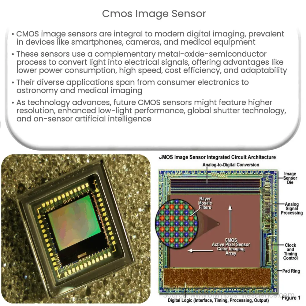
CMOS image sensors are a type of active-pixel sensor (APS) that use a complementary metal-oxide-semiconductor process to convert light into electrical signals. They consist of an array of photodiodes, each serving as an individual pixel, which capture light and produce an electrical charge proportional to the intensity of the incoming light. These charges are then converted into digital values through analog-to-digital converters (ADCs) and processed into a final image.
One of the primary advantages of CMOS sensors is that they integrate all necessary processing components, such as ADCs and amplifiers, onto the same chip as the photodiodes. This allows for faster readout speeds, reduced power consumption, and more compact designs compared to alternative technologies such as CCD (Charge-Coupled Device) sensors.
Advantages of CMOS Image Sensors
There are several benefits to using CMOS image sensors in imaging applications, including:
- Lower Power Consumption: CMOS sensors consume significantly less power than CCD sensors due to their on-chip processing capabilities. This makes them ideal for battery-powered devices such as smartphones and digital cameras.
- High Speed: The integration of ADCs and amplifiers directly on the sensor chip allows for faster readout speeds, enabling high frame rates and reduced motion blur in fast-moving scenes.
- Cost Efficiency: The CMOS fabrication process is compatible with standard semiconductor manufacturing processes, resulting in lower production costs and the ability to produce high-quality sensors at a lower price point.
- Flexibility: CMOS sensors can be easily customized for specific applications, allowing manufacturers to design sensors with unique pixel arrangements, resolutions, or other characteristics to suit their needs.
Applications of CMOS Image Sensors
Thanks to their numerous advantages, CMOS image sensors have found their way into a wide variety of applications, including:
- Digital Cameras: CMOS sensors are the primary choice for digital cameras, ranging from consumer point-and-shoot models to professional DSLRs and mirrorless cameras, due to their high image quality, speed, and cost-effectiveness.
- Smartphones: The compact size and low power consumption of CMOS sensors make them ideal for use in smartphone cameras, allowing for high-quality imaging in a small form factor.
Automotive: CMOS sensors are used in a variety of automotive applications, such as rearview cameras, lane departure warning systems, and autonomous driving systems. Their high-speed performance, durability, and low-light sensitivity make them well-suited for these demanding environments.
Future Developments and Innovations
As technology continues to advance, the capabilities of CMOS image sensors are expected to improve further. Some potential developments and innovations include:
- Higher Resolution: Researchers are continually working on increasing the resolution of CMOS sensors, enabling even greater detail in captured images. This could lead to even more precise imaging in applications such as microscopy and medical diagnostics.
- Better Low-Light Performance: Improvements in sensor design and manufacturing processes may lead to enhanced low-light sensitivity and reduced noise, allowing for better image quality in challenging lighting conditions.
- Global Shutter Technology: Most CMOS sensors currently use a rolling shutter mechanism, which can cause distortion in fast-moving scenes. The development of global shutter technology, which captures the entire image simultaneously, could eliminate this issue and further enhance the performance of CMOS sensors in high-speed applications.
- On-Sensor Artificial Intelligence: As artificial intelligence and machine learning techniques advance, it is possible that future CMOS sensors could integrate AI processing capabilities directly on the sensor chip. This would enable more sophisticated image processing, such as real-time object recognition and tracking, without the need for additional hardware or processing power.
Conclusion
CMOS image sensors have revolutionized the world of digital imaging by offering a combination of high image quality, low power consumption, and cost efficiency. They have become an indispensable component in a wide range of applications, from consumer electronics to specialized scientific and industrial equipment. As technology continues to evolve, we can expect to see even more impressive advancements in CMOS image sensor capabilities, further expanding their applications and potential impact on our lives.